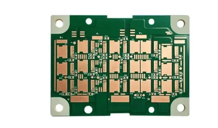
Eight-layer PCB
APPLICATION: PACKAGING TEST
Name: Eight-layer board
  • Plate thickness: 4.5mm
  • Plate: S1000-2M
  • Line width/line spacing: 8/9MIL
  • Minimum aperture: 0.4mm
  • Surface technology: Gold Deposition
  • Process characteristics: Thick copper, Plate hole metal 30U"
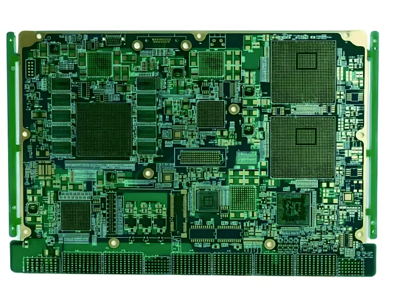
APPLICATION: INDUSTRIAL CONTROL
Name: Twenty layer plate, Four stage
  • Plate thickness: 5.5mm
  • Sheet: EM-370 (Z)
  • Line width/line spacing: 5.9/5.9mil
  • Minimum hole: 0.25mm
  • Surface technology: Whole Board Electric
  • Process characteristics: Multilayer thermoelectric separation
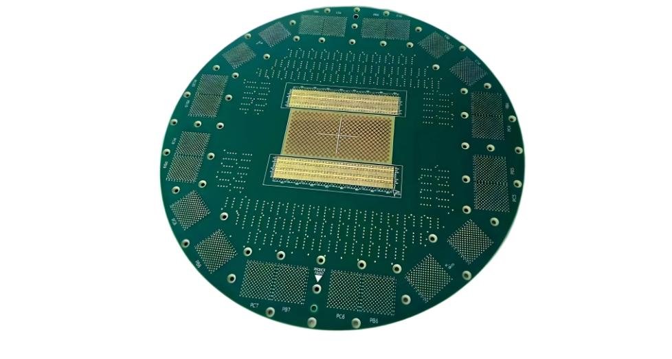
APPLICATION: AUTOMOBILE PLATE
Name: Two-layer board
  • Plate thickness: 3.8mm
  • Plate: FR4+Red Copper
  • Line width/line spacing: 3/3mil
  • Minimum hole: 0.4mm
  • Surface technology: Gold Deposition
  • Process characteristics: 4th stage HDI hole stacking
APPLICATION: MEDICAL CARE
Name: Twelve layer plate, Five stage
  • Plate thickness: 1.6mm
  • Plate: S1000-2M
  • Line width/line spacing: 6/3mil
  • Minimum hole: 0.3mm
  • Surface technology: Gold Deposition
  • Process features: 5th order arbitrary half hole, depth control & capping
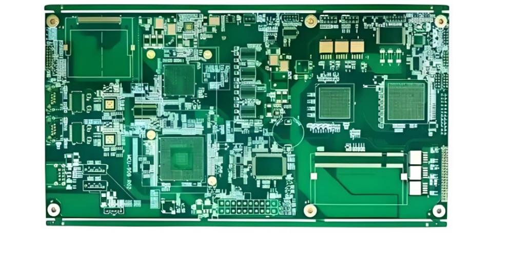
APPLICATION: INDUSTRIAL CONTROL
Name: Three-layer board
  • Plate thickness: 3.2mm
  • Plate: F4BME-1/2+Rogers4450 PP
  • Line width/line spacing: 12/14mil
  • Minimum hole: 0.6mm
  • Surface technology: Gold Deposition
  • Process features: Step plate, metal edging
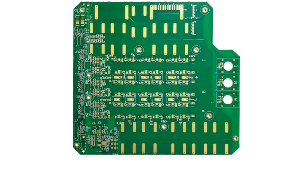
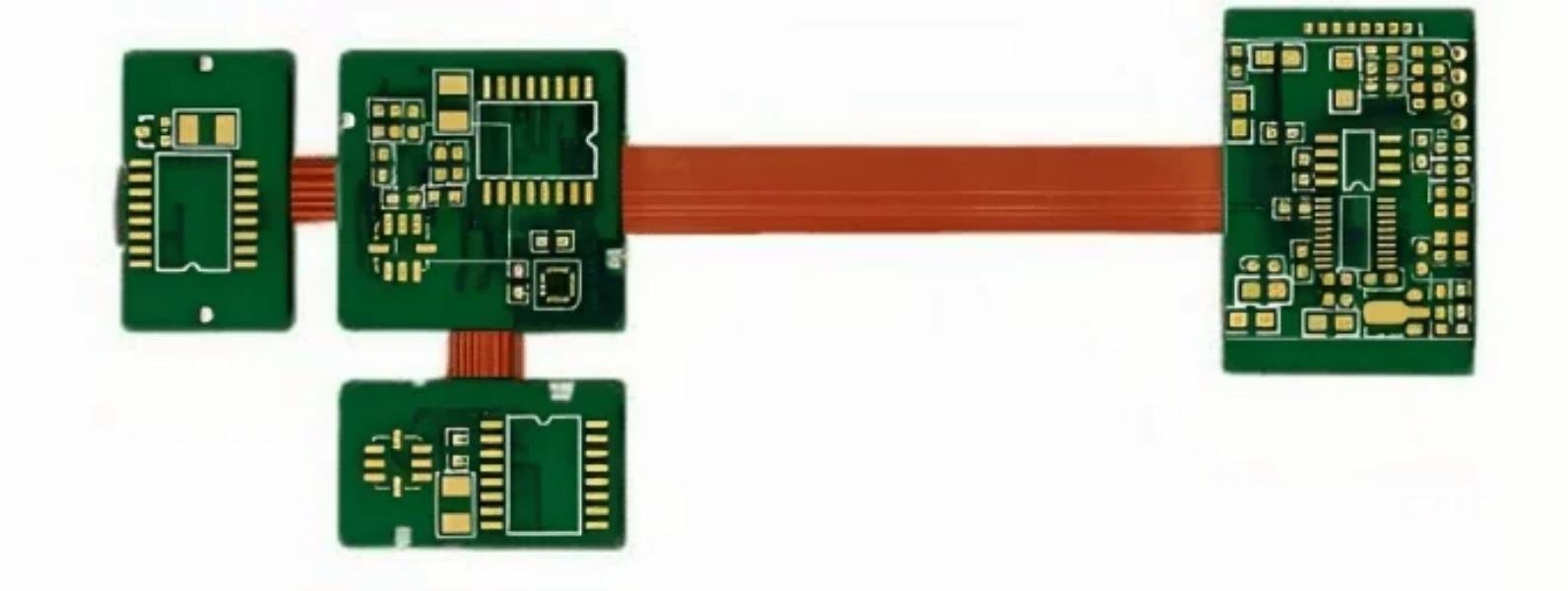
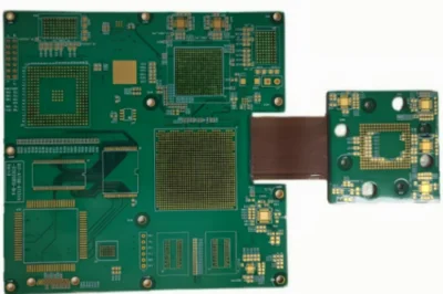
APPLICATION: SATELLITE & HIGH-FREQUENCY COMMUNICATION
Name: Four layer plate
  • Plate thickness: 1.6mm (6-layer rigid board)
  • Plate: R-F777+S1000-2M
  • Line width/line spacing: 4/4mil
  • Minimum hole: 0.2mm
  • Surface technology: Gold Deposition
  • Process characteristics: Rigid-flexible interconnection combination
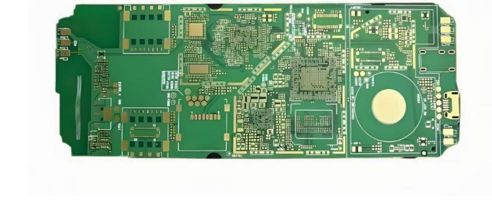
APPLICATION: MEDICAL CARE
Name: Medical Special PCB
  • Plate thickness: 1.6mm
  • Plate: S1000-2M
  • Line width/line spacing: 5/5mil
  • Minimum hole: 0.3mm
  • Surface technology: Gold Deposition
  • Process features: High-precision manufacturing
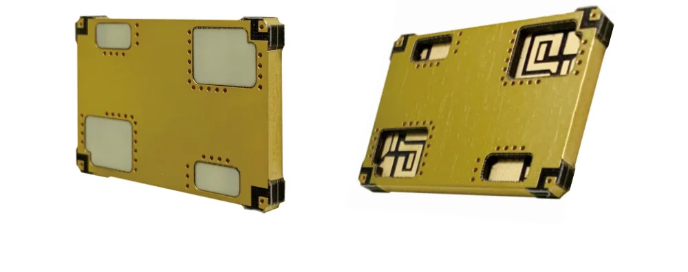
APPLICATION: INDUSTRIAL CONTROL
Name: Industrial Control PCB
  • Plate thickness: 3.0mm
  • Plate: FR4
  • Line width/line spacing: 8/8mil
  • Minimum hole: 0.4mm
  • Surface technology: Gold Deposition
  • Process features: Stable high-temperature resistance
APPLICATION: Secure Communication
Name: Secure Communication PCB
  • Plate thickness: 2.0mm
  • Plate: Rogers 4450
  • Line width/line spacing: 4/4mil
  • Minimum hole: 0.25mm
  • Surface technology: Gold Plating
  • Process features: Low loss high-frequency performance

PCBA Assembly Services

Specialized Assembly for Security, Surveillance & Industrial Electronics
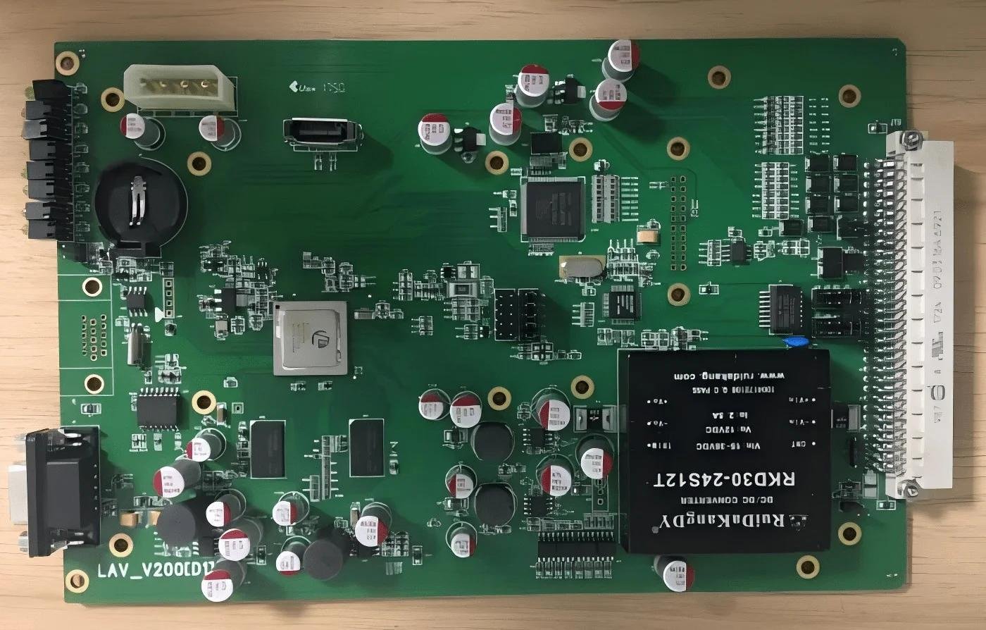
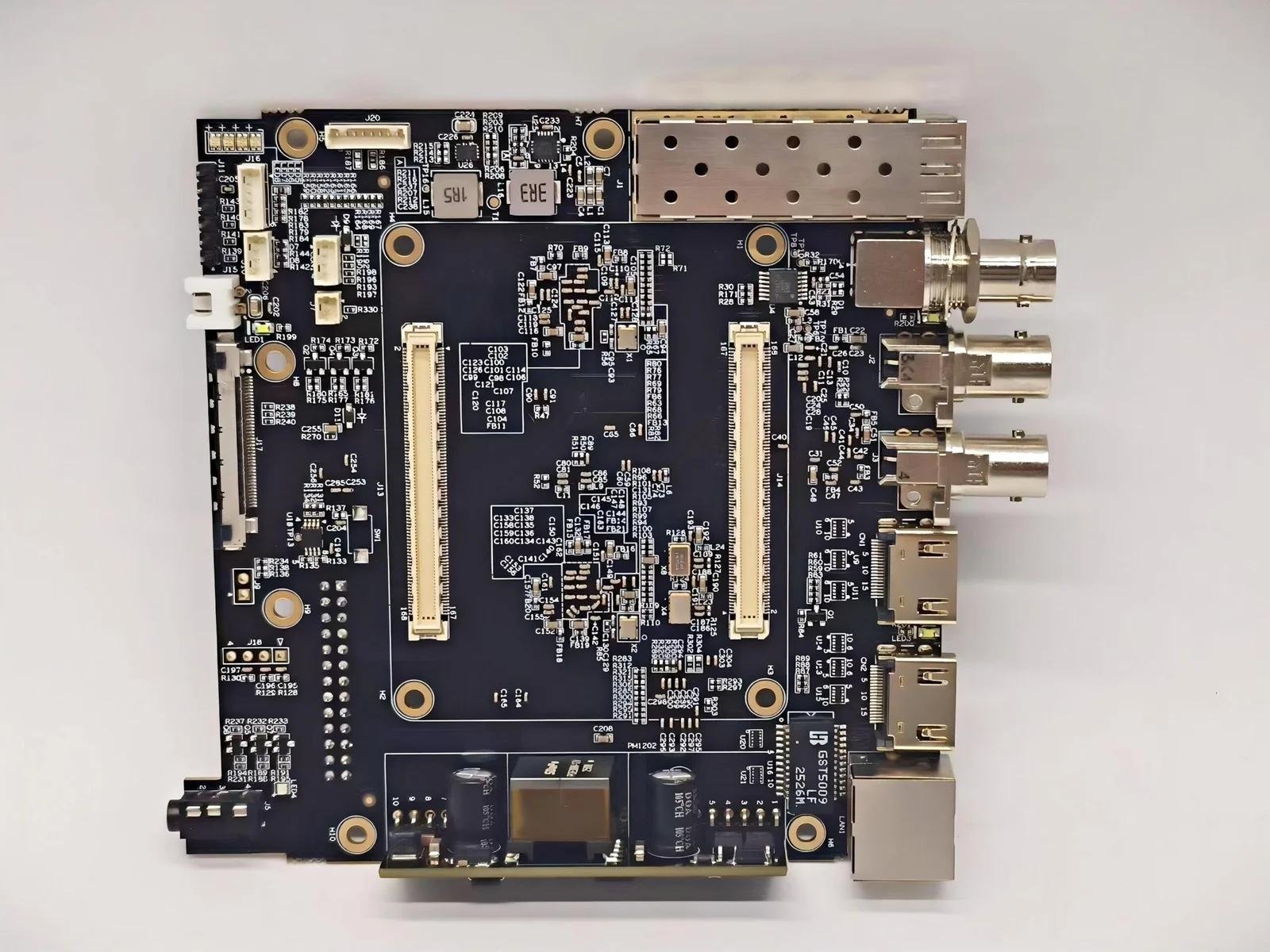
Law Enforcement Recorder PCBA
APPLICATION: LAW ENFORCEMENT
Law Enforcement Recorder Mainboard
  • High durability for field use
  • Compact design for portability
  • Stable signal transmission
Security IP Camera PCBA
APPLICATION: SECURITY MONITORING
Professional IP Camera Mainboard
  • 4K video processing support
  • Low-power for 24/7 operation
  • Anti-interference signal design
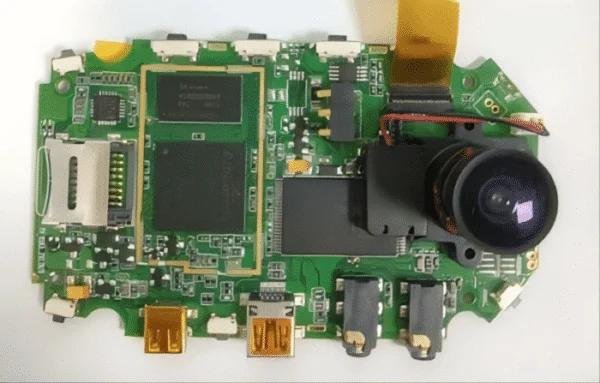
Portable IP Camera PCBA
APPLICATION: PORTABLE SURVEILLANCE
Portable IP Camera Mainboard (with Lens)
  • Integrated lens & sensor module
  • Wireless transmission capability
  • Small form factor

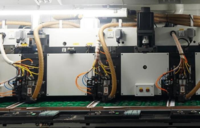
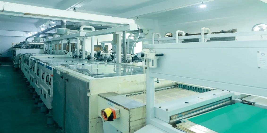
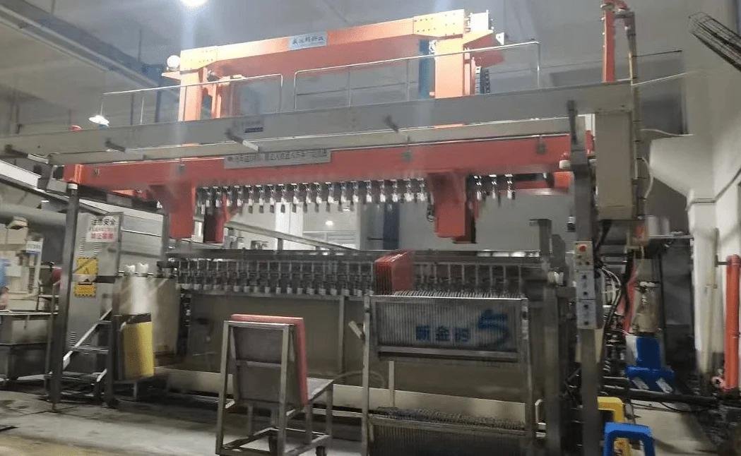
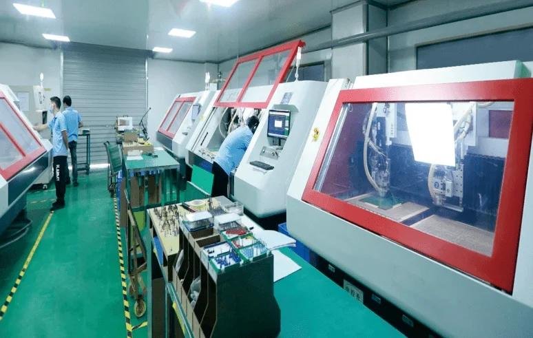
Manufacturing Equipment

State-of-the-Art Production Facilities
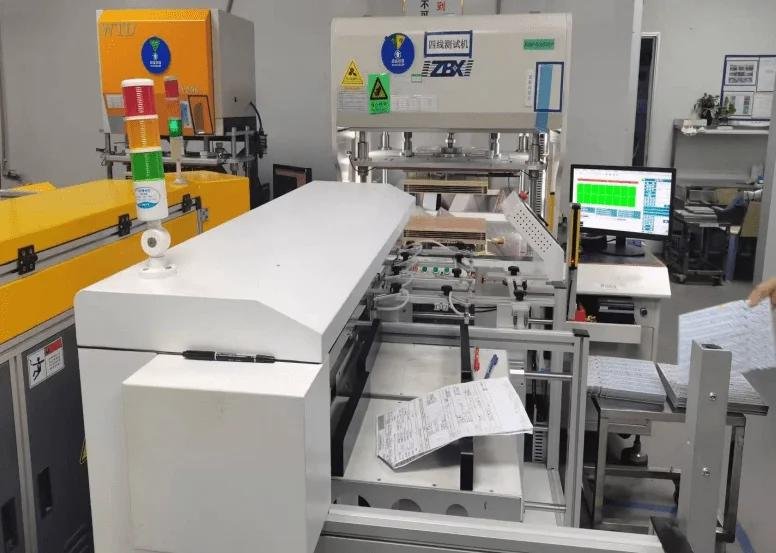
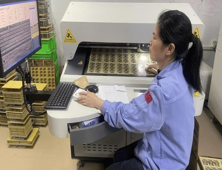
Testing Workshop
Testing Workshop
Image failed to load
Testing Workshop
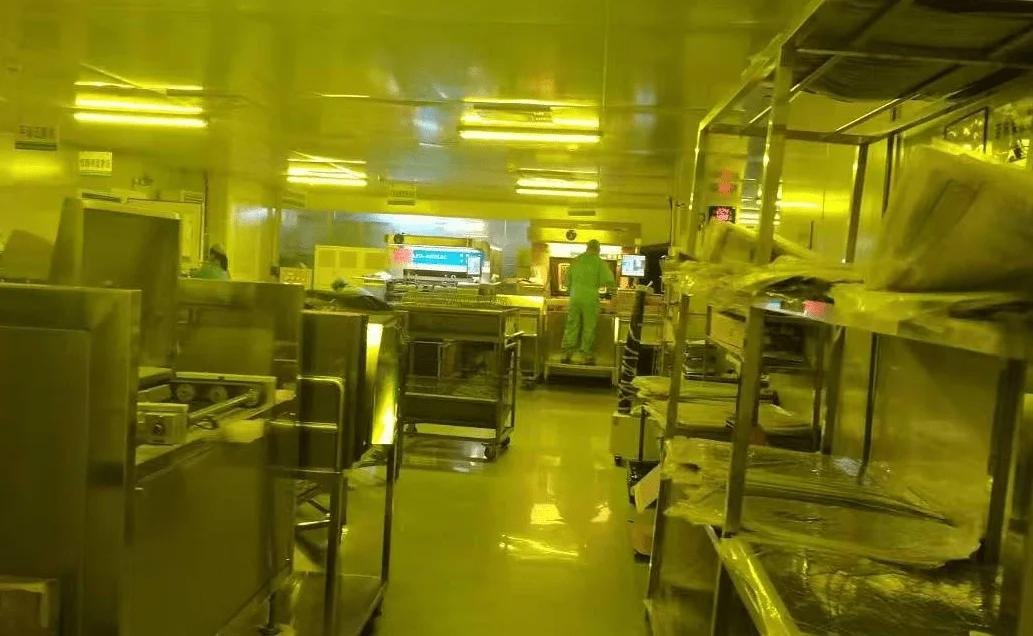
Dry Area Workshop
Dry Area Workshop
Image failed to load
Dry Area Workshop
Routing Machine
Routing Machine
Image failed to load
Routing Machine
Grinding & Solder Mask Developing Machine
Grinding & Solder Mask
Developing Machine
Grinding & Solder Mask Developing Machine
Inner Layer Workshop
Image failed to load
Inner Layer Workshop
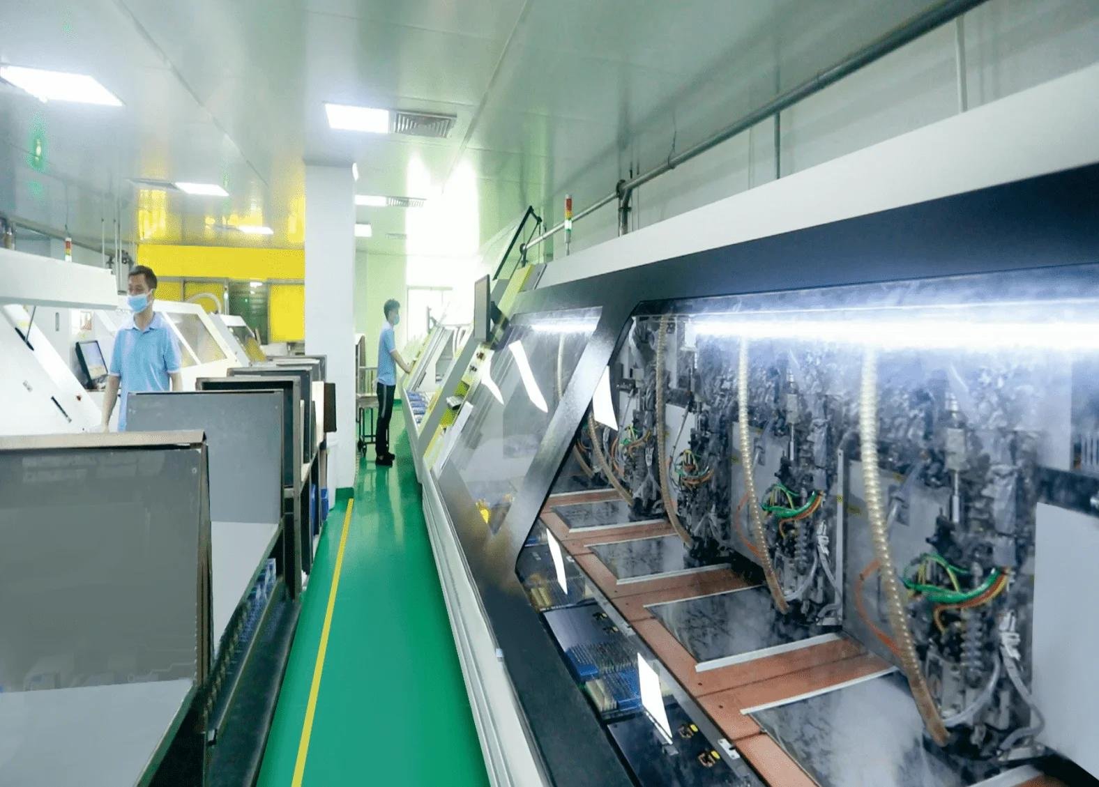
Graphic Electric Automatic Line
Graphic Electric
Automatic Line
Graphic Electric Automatic Line
Outer Shape Workshop
Image failed to load
Outer Shape Workshop
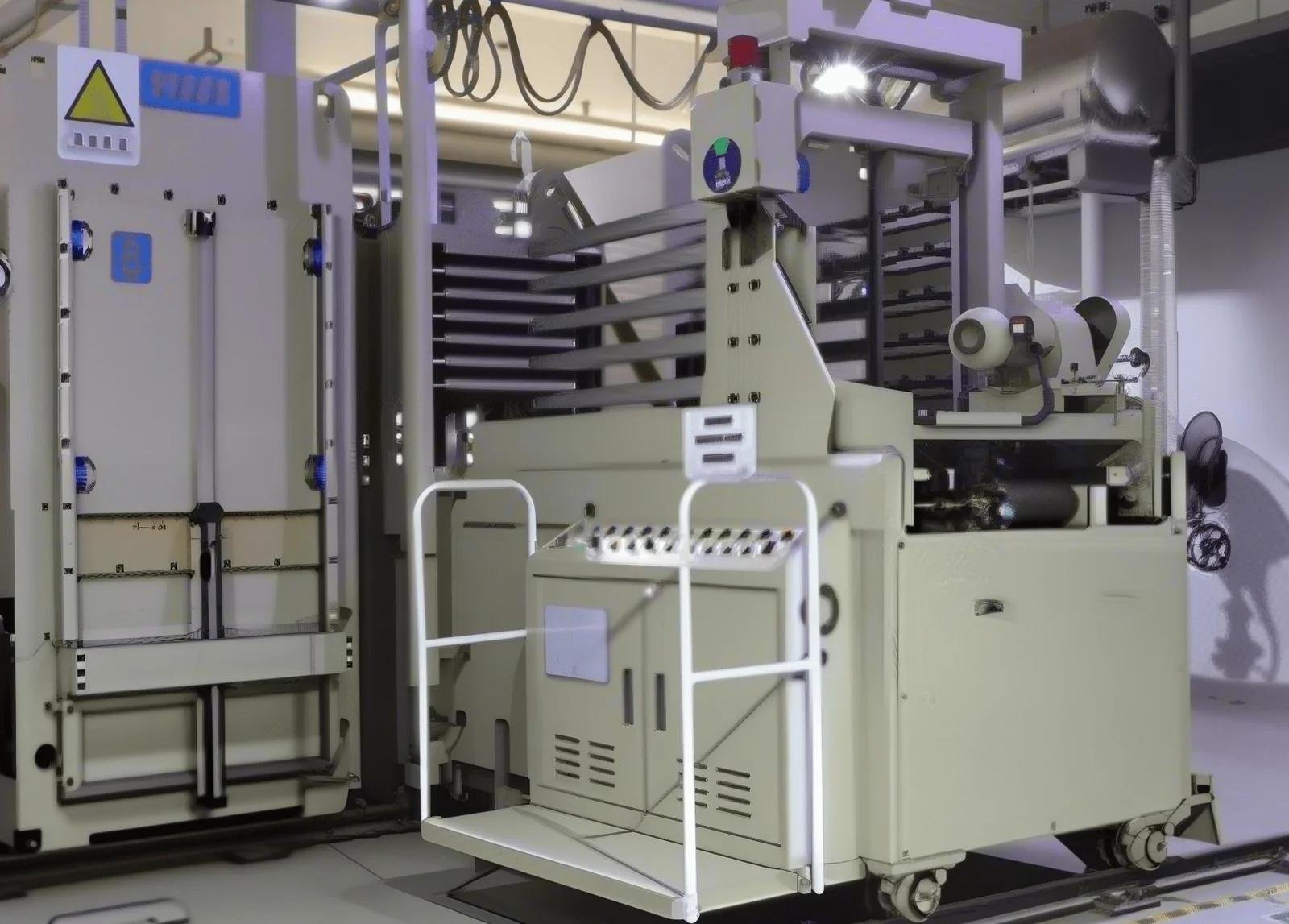
Laminating Machine
Laminating Machine
Image failed to load
Laminating Machine
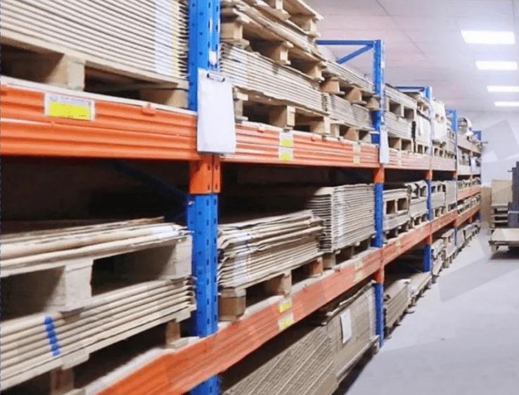
Raw Material Warehouse
Image failed to load
Raw Material Warehouse
Drilling Workshop
Drilling Workshop
Image failed to load
Drilling Workshop
Industrial Auxiliary Equipment
Industrial Auxiliary
Equipment
Industrial Auxiliary Equipment

SMT Equipment Showcase

State-of-the-Art SMT Production Line Equipment
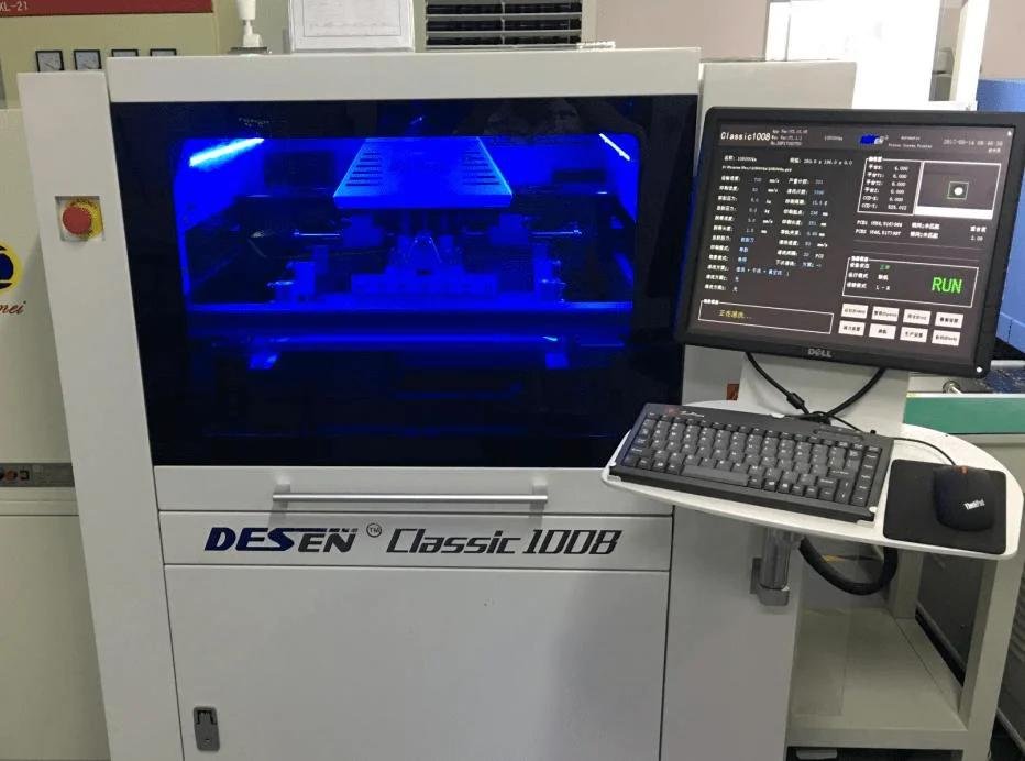
DESEN Classic 1008
DESEN Classic 1008 High-Precision Automatic Solder Paste Printer
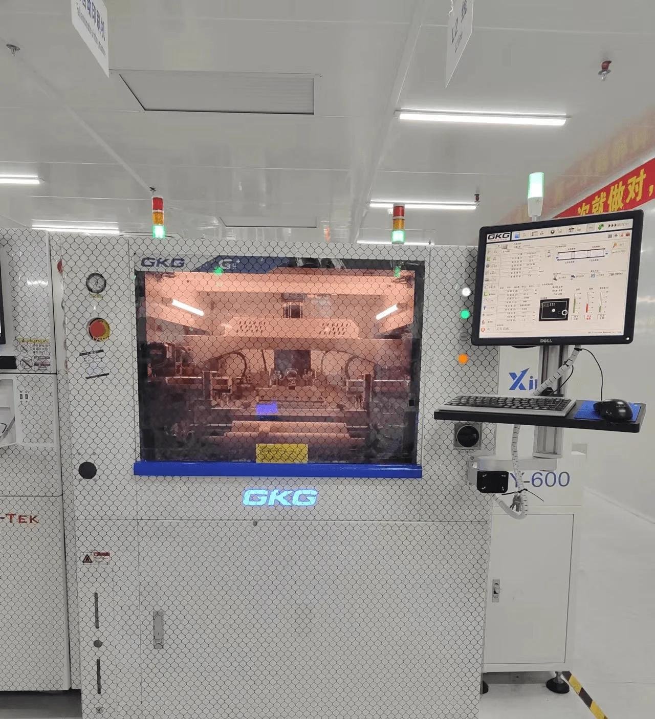
GKG G9+
GKG G9+ High-Precision Automatic Solder Paste Printer
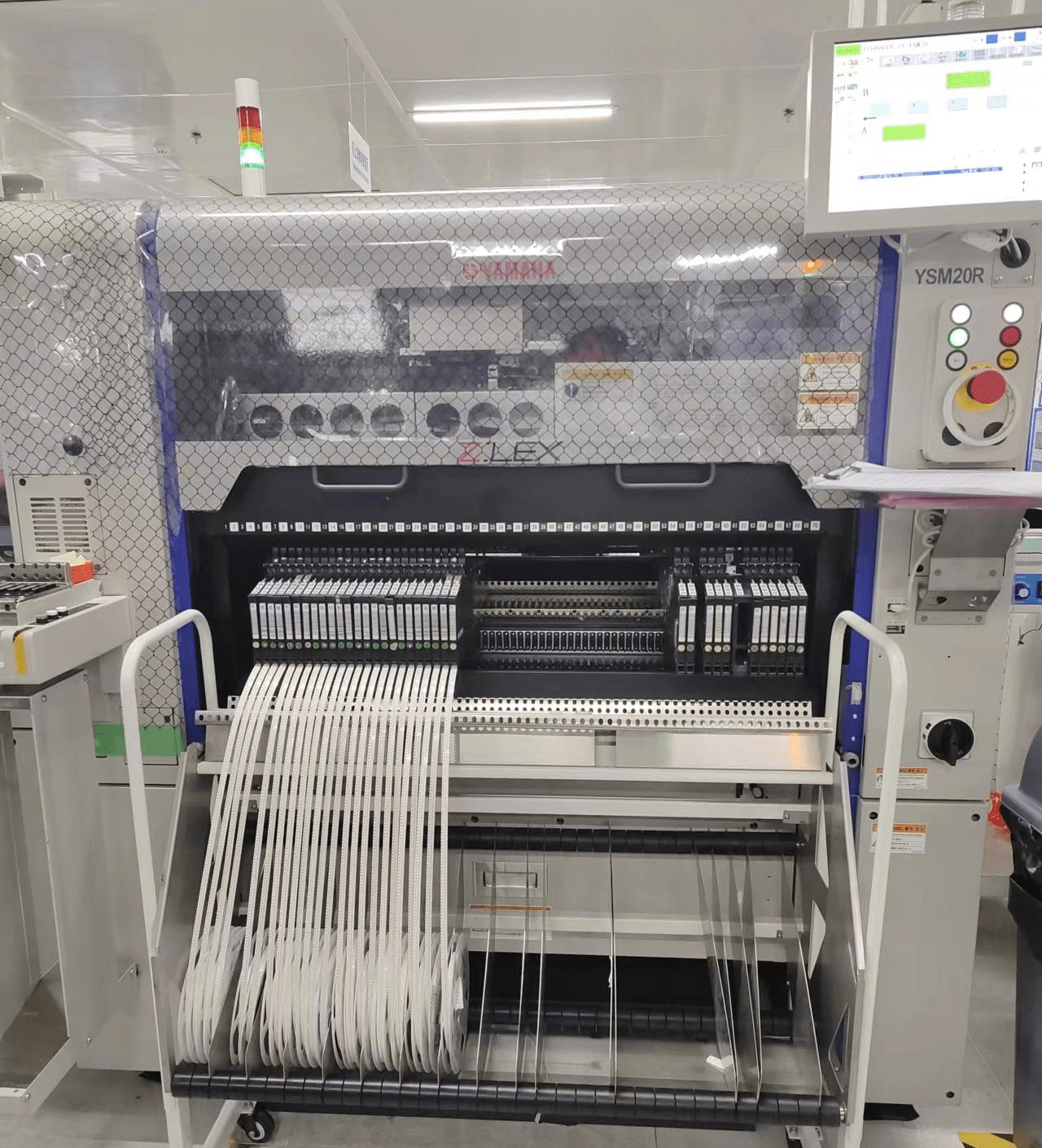
YAMAHA YSM20R
YAMAHA YSM20R High-Precision Automatic SMT Placement Machine
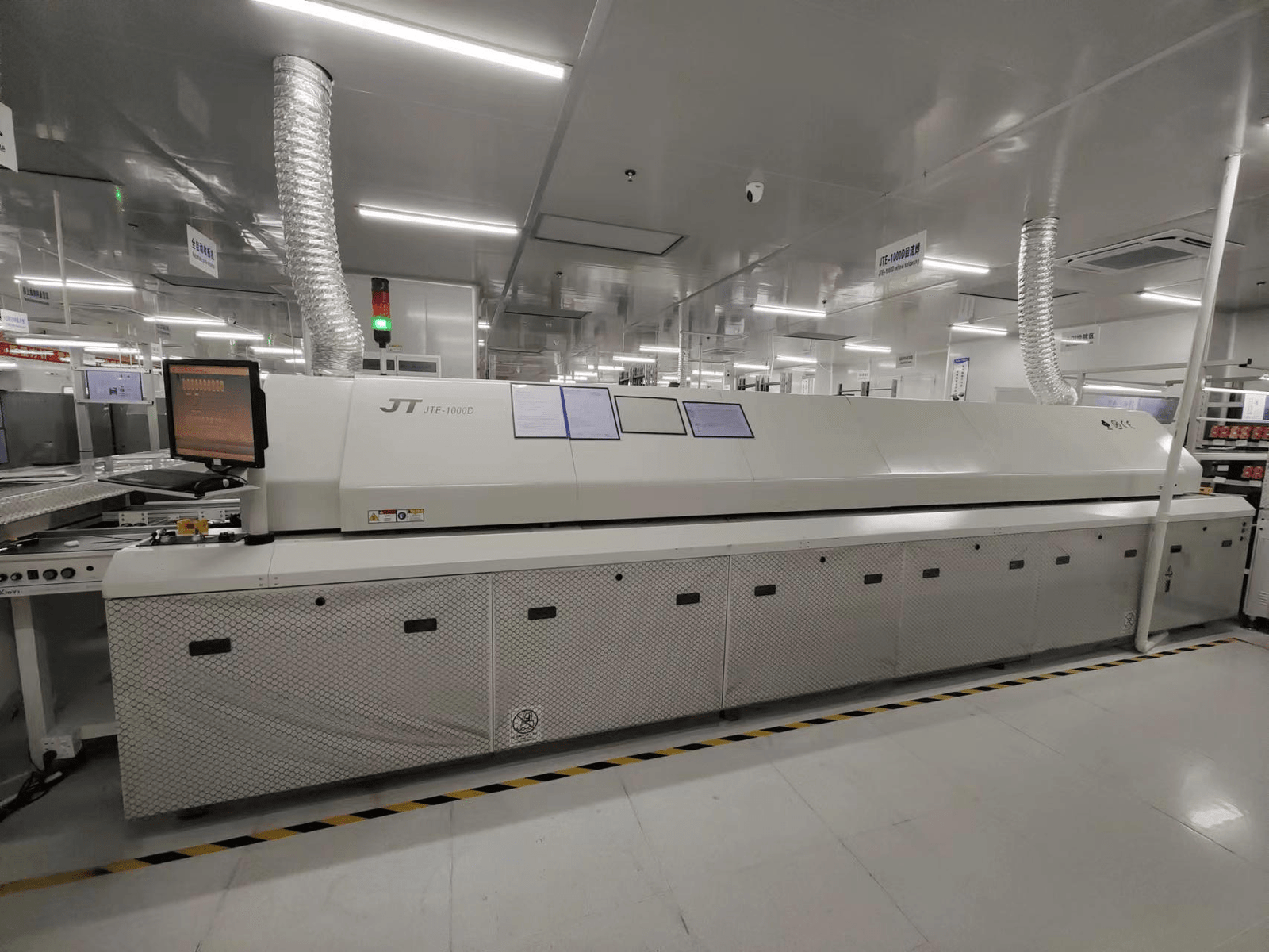
JTE-1000D
JTE-1000D 10-Zone Reflow Oven (Jietuo Brand)
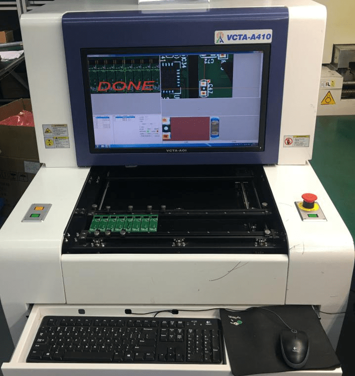
VCTA-A410
VCTA-A410 Automatic Optical Inspection (AOI) Machine (Zhenhuaxing Brand)
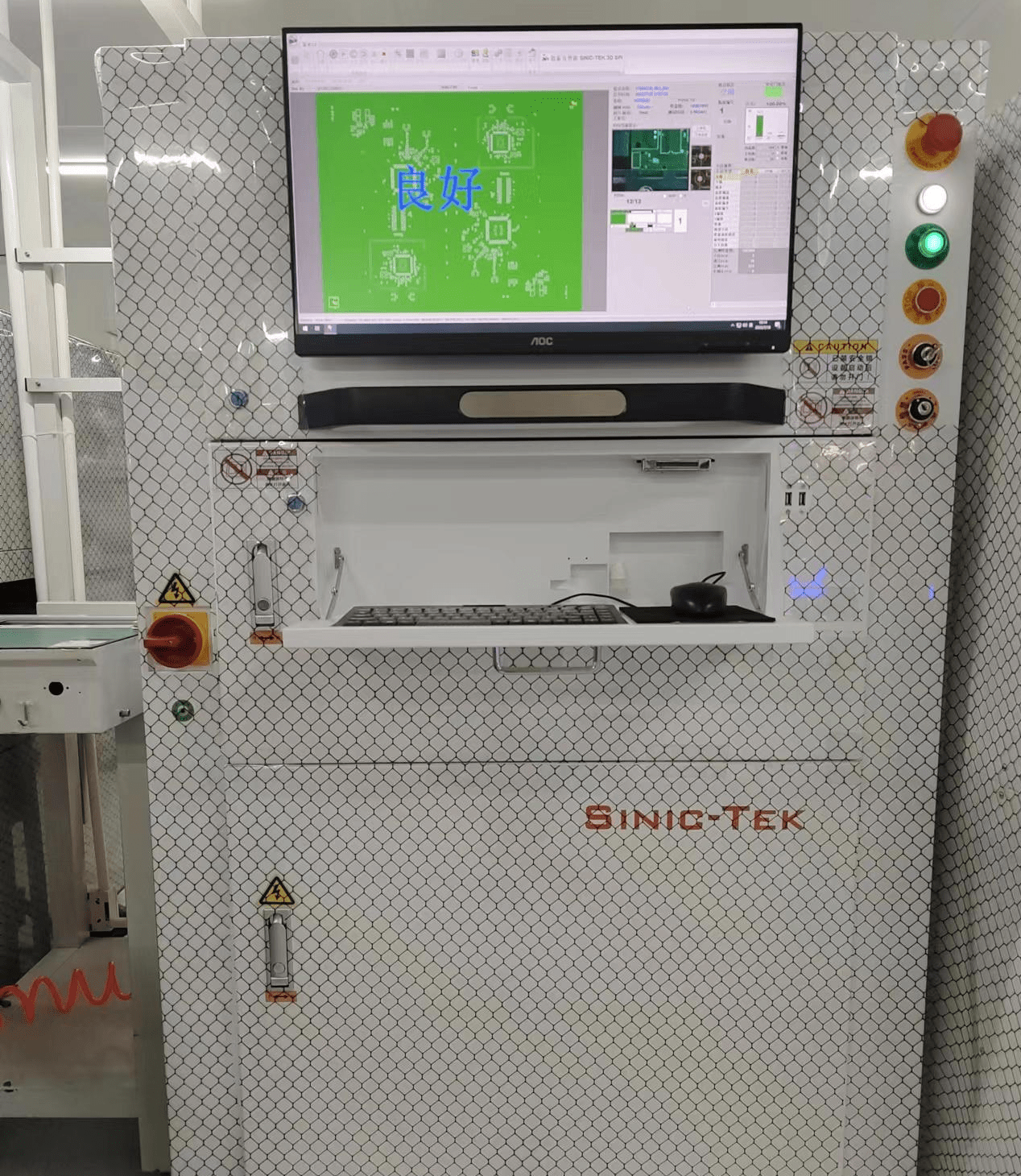
Sitaike S8030
Sitaike S8030 3D Solder Paste Inspection (SPI) Machine
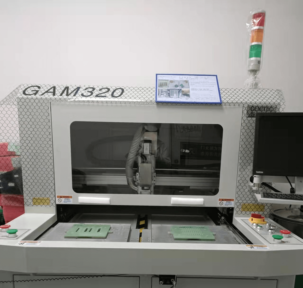
GAM320
GAM320 High-Precision PCB Depaneling Machine
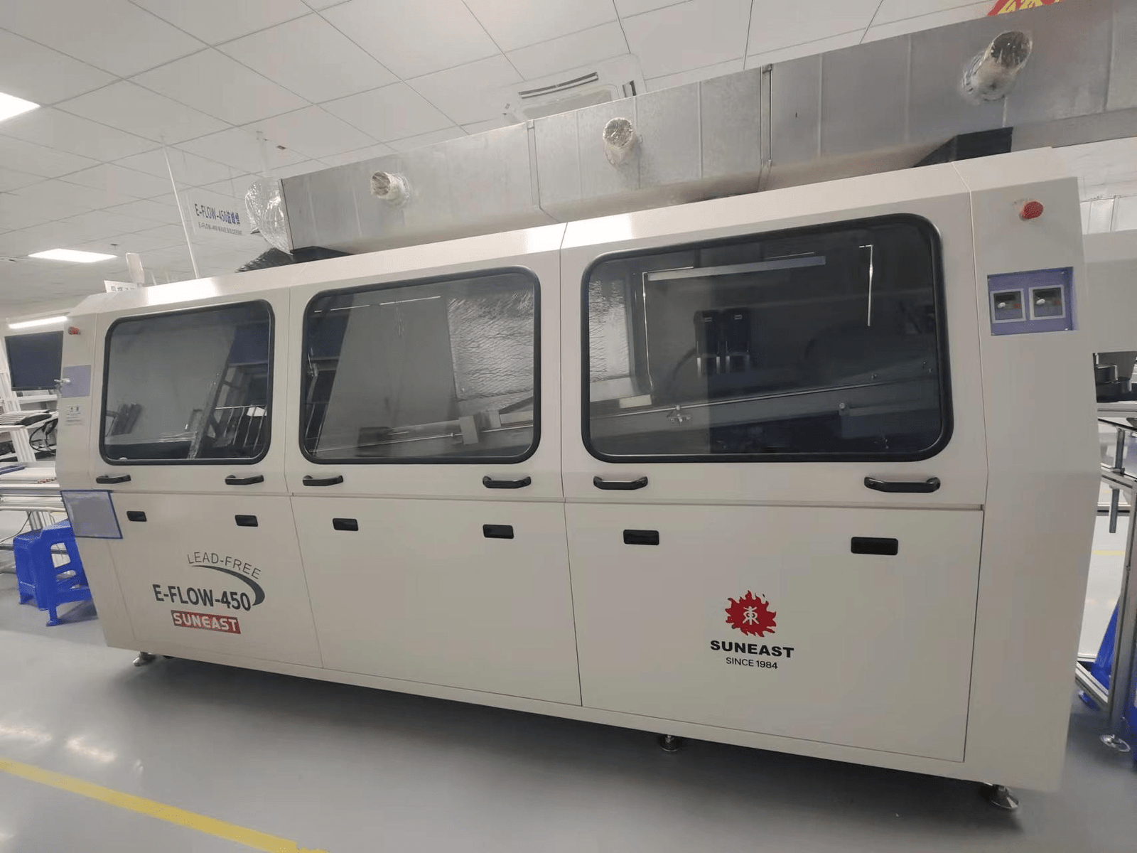
E-FLOW-450
E-FLOW-450 Wave Soldering Machine
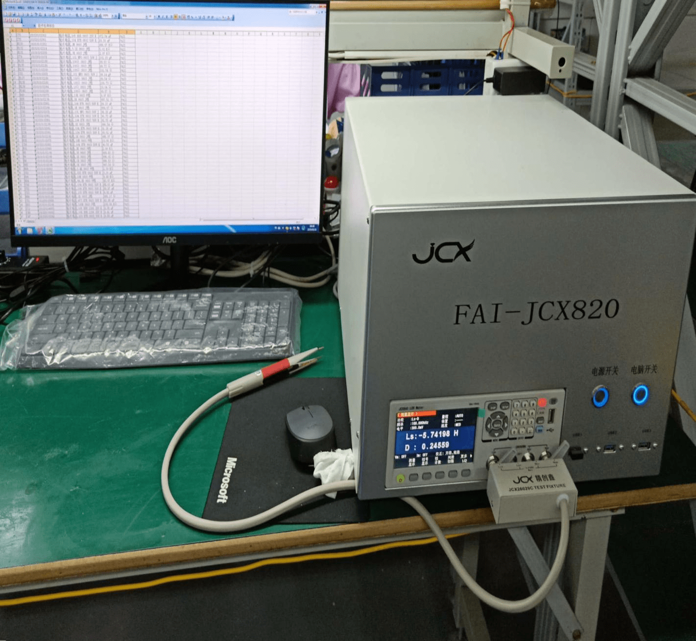
FAI-JCX820
FAI-JCX820 First Article Inspection (FAI) Tester (Jingchuangxin Brand)
×
Equipment Image

Key Specifications (From Summaries)

Product Application Fields

High-performance components for diverse industrial applications

Network Communication

Network Communication

Stable signal transmission, anti-interference design, suitable for 5G base stations, routers.

Automotive Electronics

Automotive Electronics

High temperature resistance, anti-interference, applied in vehicle navigation, autonomous driving sensors.

Automation Equipment

Automation Equipment

High precision, improves production efficiency, used for industrial robots, intelligent production lines.

Medical Electronics

Medical Electronics

High reliability, high precision, applicable to medical monitors, diagnostic equipment.

Optical Storage New Energy

Optical Storage New Energy

Efficient energy conversion, suitable for solar photovoltaic, energy storage batteries, charging piles.

Industrial Control

Industrial Control

Stable operation, compatible with PLC, frequency converters, industrial instruments.

Quality Control

Strict Standard System for PCB Quality Assurance

Raw Material Inspection

All raw materials are verified against international standards before arrangement. We cross-check material certificates to avoid hidden material risks for your projects.

In-Process Control

Unified inspection standards apply throughout all processing stages. Continuous quality tracking keeps stable and uniform board performance.

Electrical Testing

All finished PCBs go through open-short, impedance and continuity tests to reduce circuit failure risks after shipment.

Dimensional & Visual Check

Precise measurement and visual inspection cover thickness, outline, pads, solder mask and silkscreen to meet your custom specs.

Reliability Testing

Thermal shock, solderability and environmental tests are available to support industrial and automotive electronic applications.

Final Pre-Shipment Audit

Every order is fully reviewed before delivery. We recheck technical specs, packaging and order details to match your quality requirements.

Process Capability

Precision Manufacturing Standards

Layer1-60Layers
MaterialFR4,HTC, halogen free, metal substrate, high frequency material, High Speed Material, High CTI
Board thickness0.4mm-8.0mm
Min board size10×10mm
Max board size622mm×1200mm
Board thickness tolerance≤1.0mm, +/-0.1mm; ≥1.0mm, +/-10%
Copper Thickness0.33oz-30oz
Min Trace Width2mil(0.05mm)
Min Spacing2mil(0.05mm)
Min Drilling Dia0.10mm
PTH copper thickness0.4-2mil(10-50um)
Line width tolerance±20%
V-cut angle25°, 30°, 45°, 60°
Peel Strength of Line≥6lb/in(≥107g/mm)
Impedance control and tolerance±10%
Twist & Warp≤ 0.75%
Soldermask ColorGreen, Red, Blue, White, Black, Yellow
Surface Finish/PlatingChemical gold plating, gold plating, chemical tin plating, chemical silver plating, anti-oxidation treatment and tin spraying, electroplated gold finger, NiPdAu
Maximum Aspect Ratio25:1
Hole TypesThrough hole, blind hole, buried hole, counterbore, PTH pan hole, Backdrill, Step hole

Product Delivery Date

Efficient and Reliable PCB Delivery Schedule

Sample Processing TimeBatch Processing Time
TypeFastest DeliveryNormal DeliveryTypeDelivery Date
Double Sided Board24 Hours3 DaysDouble Sided Board7 Days
4-Layer Laminate36 Hours5 Days4-Layer Laminate10 Days
6-Layer Laminate48 Hours6 Days6-Layer Laminate12 Days
8-Layer Laminate72 Hours7 Days8-Layer Laminate12 Days
10-Layer Laminate4 Days9 Days10-Layer Laminate14 Days
12-Layer Laminate4 Days11 Days12-Layer Laminate16 Days
14-Layer Laminate5 Days13 Days14-Layer Laminate16 Days
16-Layer Laminate5 Days15 Days16-Layer Laminate18 Days
18 Layers & AboveTo Be NegotiatedTo Be Negotiated18 Layers & Above18 Days
Scroll to Top